Flip-Flops: Adding Memory to Digital Circuits
Introduction
Everything we've learned so far—gates, MUXes, decoders—are combinational circuits. Their outputs depend only on current inputs, with no memory of the past. But real digital systems need memory:
- CPUs need to remember instructions
- Counters need to track values
- State machines need to remember which state they're in
- Registers need to store data
Enter flip-flops: the fundamental memory elements of digital systems.
The flip-flop is arguably one of the most important inventions in electronics. Without it, we wouldn't have:
- Computers (no way to store programs or data)
- Digital clocks (no way to count time)
- Sequential logic (no state machines)
- Modern digital communication
Every bit in your computer's RAM is stored in a flip-flop or similar memory cell!
From Combinational to Sequential Logic
The Key Difference
| Combinational | Sequential |
|---|---|
| Output = f(current inputs) | Output = f(current inputs, past inputs) |
| No memory | Has memory |
| Asynchronous (immediate) | Often synchronous (clocked) |
| Examples: AND, OR, MUX | Examples: flip-flop, counter, register |
Sequential Circuit Structure:
[Diagram showing:
- Inputs →
- Combinational Logic block
- → Outputs
- Memory Elements (flip-flops)
- Feedback loop from memory back to combinational logic
- Clock signal feeding into memory elements]
The SR Latch: Building Block of Memory
Before flip-flops, let's understand latches—the simpler, asynchronous cousins.
SR Latch (Set-Reset Latch)
The SR latch is the most basic memory element, built from cross-coupled NOR or NAND gates.
SR Latch Using NOR Gates
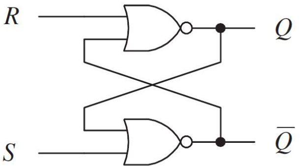
Truth Table:
| S | R | Q(next) | Q̄(next) | Action |
|---|---|---|---|---|
| 0 | 0 | Q | Q̄ | Hold (maintain current state) |
| 1 | 0 | 1 | 0 | Set (Q becomes 1) |
| 0 | 1 | 0 | 1 | Reset (Q becomes 0) |
| 1 | 1 | X | X | Invalid (forbidden state) |
Operation:
- Set (S=1, R=0): Forces Q=1, Q̄=0
- Reset (S=0, R=1): Forces Q=0, Q̄=1
- Hold (S=0, R=0): Q maintains its previous value (memory!)
- Invalid (S=1, R=1): Both outputs try to go to 0, contradicts Q and Q̄ relationship
When both S and R are 1, the outputs become unpredictable when S and R return to 0. This race condition makes the SR latch unreliable in some applications. Solution: Use JK flip-flop (coming later) or ensure S and R are never both 1.
SR Latch Using NAND Gates
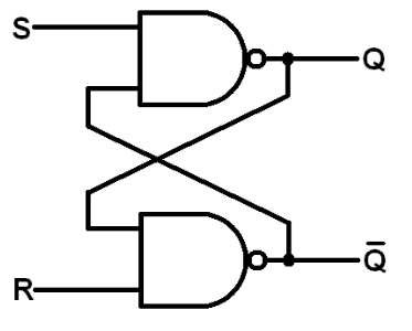
Truth Table (active-low inputs):
| S̄ | R̄ | Q | Q̄ | Action |
|---|---|---|---|---|
| 1 | 1 | Q | Q̄ | Hold |
| 0 | 1 | 1 | 0 | Set |
| 1 | 0 | 0 | 1 | Reset |
| 0 | 0 | 1 | 1 | Invalid |
This version is more common because NAND gates are often easier to implement than NOR.
D Latch: Data Latch
The D latch (Data latch or Delay latch) solves the SR=11 problem by using only one data input.
D Latch Structure
Truth Table:
| E | D | Q(next) | Action |
|---|---|---|---|
| 0 | X | Q | Hold (ignore D) |
| 1 | 0 | 0 | Reset Q to 0 |
| 1 | 1 | 1 | Set Q to 1 |
Operation:
- Enable=0: Output Q holds previous value (memory)
- Enable=1: Output Q follows input D (transparent)
Characteristic Equation:
When Enable=1, the D latch is "transparent"—Q immediately follows D. This can be problematic in synchronous systems because any glitch on D affects Q. Solution: Use edge-triggered flip-flops instead of level-triggered latches.

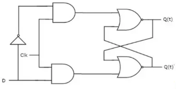
Edge-Triggered Flip-Flops
Latches are level-triggered (respond while Enable=1). Flip-flops are edge-triggered (respond only at clock edge—rising or falling).
Advantages of Edge-Triggering:
- Synchronous operation: All flip-flops change simultaneously
- Noise immunity: Ignores glitches except at clock edge
- Predictable timing: Easier to design reliable systems
- Avoids race conditions: Input changes between clock edges don't matter
Clock Edges
Rising Edge (Positive Edge): Transition from 0 to 1
Falling Edge (Negative Edge): Transition from 1 to 0

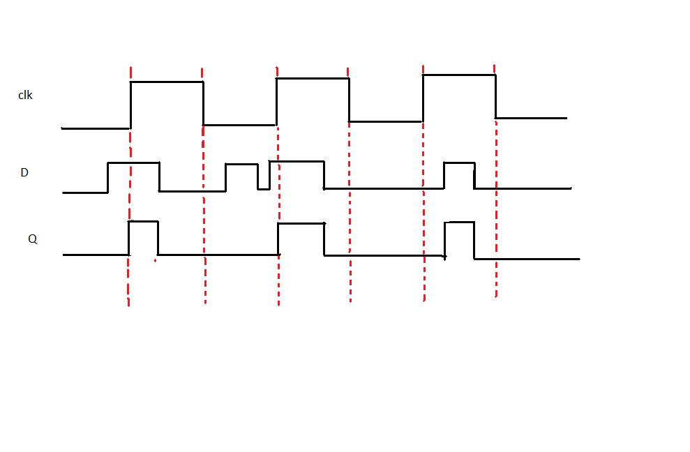
D Flip-Flop: Most Common Flip-Flop
The D flip-flop (Data or Delay flip-flop) is the workhorse of digital systems. It captures the D input value at the clock edge and holds it until the next clock edge.
D Flip-Flop Symbol

Symbol Variations:
- > at CLK: Rising-edge triggered
- >○ at CLK: Falling-edge triggered (bubble = inversion)
D Flip-Flop Truth Table
| CLK | D | Q(next) | Q̄(next) |
|---|---|---|---|
| ↑ | 0 | 0 | 1 |
| ↑ | 1 | 1 | 0 |
| No edge | X | Q | Q̄ |
Characteristic Equation:
Simple! Q becomes whatever D was at the clock edge.
Critical Timing Parameters
1. Setup Time (tsu)
- Minimum time D must be stable BEFORE clock edge
- Typical: 1-5 ns for modern logic
2. Hold Time (th)
- Minimum time D must remain stable AFTER clock edge
- Typical: 0-2 ns
3. Clock-to-Q Propagation Delay (tpd)
- Time from clock edge to Q output changing
- Typical: 2-10 ns
4. Maximum Clock Frequency (fmax)
- Highest frequency the flip-flop can reliably operate at
- Limited by tpd and internal delays

If D changes during setup/hold time (setup/hold violation), the flip-flop can enter a metastable state—Q becomes unpredictable! Always check timing in designs.
D Flip-Flop Applications
1. Data Storage Registers
Multiple D flip-flops in parallel = Register
8 D flip-flops = 8-bit register
2. Delay Elements
Q follows D after one clock cycle delay
Used in pipelining, synchronization
3. Shift Registers
Connect Q of one flip-flop to D of next
Data shifts through chain on each clock
4. Frequency Division
Connect Q̄ back to D
Output toggles every clock cycle = divide-by-2
JK Flip-Flop: The Universal Flip-Flop
The JK flip-flop is the most versatile flip-flop. It eliminates the SR=11 invalid state problem.
JK Flip-Flop Symbol

JK Flip-Flop Truth Table
| CLK | J | K | Q(next) | Action |
|---|---|---|---|---|
| ↑ | 0 | 0 | Q | Hold (no change) |
| ↑ | 0 | 1 | 0 | Reset |
| ↑ | 1 | 0 | 1 | Set |
| ↑ | 1 | 1 | Q̄ | Toggle (flip) |
Characteristic Equation:
Key Feature: When J=K=1, Q toggles (flips). This is why JK has no invalid state!

JK Flip-Flop Applications
1. Toggle Mode (J=K=1)
- Frequency dividers
- Counters
- Binary ripple counters
2. Configurable Operation
- Can act as D flip-flop: J=D, K=D̄
- Can act as T flip-flop: J=K=T
3. State Machines
- Flexible state transitions
T Flip-Flop: Toggle Flip-Flop
The T flip-flop (Toggle flip-flop) has one input that controls toggling.
T Flip-Flop Symbol

T Flip-Flop Truth Table
| CLK | T | Q(next) | Action |
|---|---|---|---|
| ↑ | 0 | Q | Hold (no change) |
| ↑ | 1 | Q̄ | Toggle (flip) |
Characteristic Equation:

T Flip-Flop from JK
Easy conversion: Connect J and K together!
JK flip-flop with J=K=T → T flip-flop
T Flip-Flop Applications
1. Frequency Division
T=1, connect Q̄→D: Divide-by-2 counter
Cascade multiple: Divide-by-4, 8, 16...
2. Binary Counters
Chain of T flip-flops = Ripple counter
3. Clock Generation
Generate lower frequency clocks from high-frequency source
Asynchronous Inputs: Preset and Clear
Most flip-flops have asynchronous (not clock-dependent) control inputs:
Preset (PRE) / Set: Forces Q=1 immediately, regardless of clock
Clear (CLR) / Reset: Forces Q=0 immediately, regardless of clock

Truth Table Including Async Inputs:
| PRĒ | CLR̄ | CLK | D | Q | Q̄ | Action |
|---|---|---|---|---|---|---|
| 0 | 1 | X | X | 1 | 0 | Preset (force Q=1) |
| 1 | 0 | X | X | 0 | 1 | Clear (force Q=0) |
| 0 | 0 | X | X | 1 | 1 | Invalid (both forced) |
| 1 | 1 | ↑ | D | D | D̄ | Normal operation |
- System reset: Clear all flip-flops to known state at power-up
- Emergency override: Force specific state regardless of clock
- Initialization: Set flip-flops before starting operation
Be careful: Asynchronous inputs can cause timing problems if not used properly!
Master-Slave Flip-Flops
Early flip-flop designs used master-slave architecture to achieve edge-triggering:
Structure:
- Master latch: Captures input when CLK=1
- Slave latch: Transfers master's output when CLK=0
- Output changes only during CLK transition

Advantage: True edge-triggered operation
Disadvantage: 1s catching problem (now solved with better designs)
Modern flip-flops use improved edge-detection circuits, not master-slave.
Flip-Flop Comparison Summary
| Type | Inputs | Toggle? | Common Use | Complexity |
|---|---|---|---|---|
| SR | S, R | No | Basic latch, rare in modern designs | Simple |
| D | D | No | Data storage, registers, most common | Simple |
| JK | J, K | Yes (J=K=1) | Versatile, counters | Moderate |
| T | T | Yes (T=1) | Frequency division, counters | Simple |
Selection Guide:
- Need to store data? → D flip-flop
- Need to toggle? → T flip-flop
- Need flexibility? → JK flip-flop
- Building asynchronous circuit? → SR latch
In modern digital design (FPGA, ASIC), D flip-flops dominate. Tools synthesize other types from D flip-flops if needed. Focus on understanding D flip-flops well!
Practical Circuit: 4-Bit Register
Let's build something useful: a 4-bit parallel-load register.

Operation:
- On each clock rising edge, all four flip-flops capture their D inputs simultaneously
- Outputs hold values until next clock edge
- If CLR activated, all outputs go to 0
Verilog Code Example:
// 4-bit register in Verilog
module register_4bit (
    input clk,
    input [3:0] D,
    output reg [3:0] Q
);
    always @(posedge clk) begin
        Q <= D;  // Capture D on rising edge
    end
endmodule
Applications:
- CPU registers (accumulator, program counter)
- Buffer storage
- Interface between systems
- Pipeline stages
Flip-Flop Timing Analysis
Setup and Hold Time Requirements
For reliable operation:
Where:
- T_CLK = Clock period
- t_pd(logic) = Propagation delay through combinational logic
- t_su = Setup time of flip-flop
- t_CLK skew = Clock distribution delay variations
Example Calculation:
Given:
- Combinational logic delay: 15 ns
- Flip-flop setup time: 2 ns
- Clock skew: 1 ns
Minimum clock period:
Maximum frequency:
Metastability
When setup/hold times are violated, flip-flops can enter metastable state:
- Output voltage between valid logic levels
- Takes unpredictable time to resolve to 0 or 1
- Can propagate errors through system
Solutions:
- Use synchronizers (two flip-flops in series)
- Increase clock period to meet timing
- Use faster logic families
- Proper timing analysis during design

Summary
Flip-flops are the memory elements that make digital systems possible:
✅ SR Latch: Basic memory, has invalid state
✅ D Latch: Level-triggered, transparent when enabled
✅ D Flip-Flop: Edge-triggered, most common, stores one bit
✅ JK Flip-Flop: Universal, can toggle
✅ T Flip-Flop: Simple toggle, great for counters
Key Takeaways:
- Latches: Level-triggered, asynchronous
- Flip-Flops: Edge-triggered, synchronous
- Timing: Setup and hold times are critical
- D Flip-Flop: Industry standard, simple and reliable
- Applications: Registers, counters, state machines
Now that we have memory elements, we can build counters—circuits that count clock pulses and generate sequences. This leads to state machines, timers, and more complex sequential logic!
Further Reading
- Datasheet study: 74HC74 (Dual D flip-flop)
- Clock domain crossing and metastability
- Timing analysis tools in FPGA design
- Flip-flop-based SRAM cells
Practice Problems:
- Design a divide-by-4 counter using T flip-flops
- Convert JK flip-flop to D flip-flop (find J and K in terms of D)
- Calculate maximum clock frequency given tpd=5ns, tsu=1ns, tskew=0.5ns
- Draw timing diagram for D flip-flop with changing D and CLK
- How many D flip-flops needed for 16-bit register?
- Design a switch debouncer using SR latch
- Explain why D latch is "transparent" and why it's problematic